
Articles
Custom designed processing for improved PSD performance, part I
The PSDs within SiTek's standard product range are well known for their excellent performance with high linearity, great resolution and high speed. However, like all standard devices, these PSDs have been developed to fit a wide range of applications, something that necessarily leads to compromises when it comes to parameter optimisation. By optimising the manufacturing process for a specific application, the PSD performance can be enhanced further, giving a higher value product for the customer.
Resolution
One of the great advantages of a PSD, compared to other position sensing devices, e.g. CCD and quad detectors, is the superior resolution. The resolution in a PSD is, like in other analogue devices, determined by the signal-to-noise ratio. Hence, to get as high resolution as possible the signal should be maximised while the noise should be at a minimum level.
Responsivity
Since the signal, i.e. the photo current, is set by the responsivity one would like to have as high responsivity as possible for the wavelength used. At SiTek we have developed three different processes optimised for different wavelength regions, UV (200 nm - 500 nm), Standard (500 nm - 900 nm) and YAG (900 nm - 1100 nm). By choosing the process that fits the application best the first step towards world class resolution is taken.
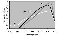
Figure 1. Spectral responsivity for detectors manufactured in different SiTek processes.
Next step is to tune the process for the specific wavelength used in the application. This is done by optimising the different layers building up the anti-reflection (AR) coating. By minimising the reflectivity the resopnsivity can be increased by almost 100 % for some wavelengths.
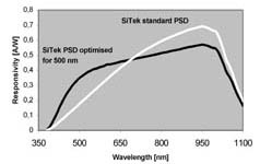
Figure 2. Spectral responsivity for SiTek detectors manufactured with different AR coating.
Noise
The noise in the PSD mainly consists of two parts, the so-called Johnson noise, generated by the inter electrode resistance, and the so-called shot noise, generated by the photocurrent in the PN-junction. For medium and high photocurrents the shot noise dominates, giving limited possibilities for optimisation but for low currents the contribution from the Johnson noise has a great influence on the total noise current. Hence, in applications with limited access of light, an optimisation of the inter electrode resistance will reduce the noise significantly and in that way improve the resolution.
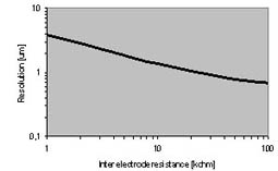
Figure 3. Resolution on a 10 mm SiTek PSD with a photo current of 1 uA and a bandwidth of 10 kHz.
These were a only few examples of the parameters which can be optimised to get an improved PSD performance. In the next edition of Non-contact we will give you some more examples, e.g. speed and reflectivity.
Custom designed processing for improved PSD performance, part II
The PSDs within SiTek's standard product range are well known for their excellent performance with high linearity, great resolution and high speed. However, like all standard devices, these PSDs have been developed to fit a wide range of applications, something that leads to necessary compromises when it comes to parameter optimisation. By optimising the manufacturing process for a specific application, the PSD performance can be enhanced further, giving a higher value product for the customer.
Reflectivity
As stated in Non-Contact 2/01, the main advantage of optimising the AR coating for a certain wavelength is that it optimises the responsivity. But even when you have a lot of light and can manage with a lower responsivity there is an important reason to use an AR coating optimised for the specific wavelength.
When the light hits the PSD surface some of the light will be reflected. When this reflected light hits other surrounding surfaces it might be reflected back on to the PSD causing errors in the measurement. With an optimised AR coating the reflected light is kept well below 2 % of the incoming light, which eliminates the cause of secondary reflections.
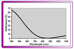
Figure 1. Spectral reflectivity for SiTek detector with AR coating optimised for 850 nm.
Speed
With todays fast electronics, the demand for high speed devices increases. Even though the PSD, due to its simple design, is much faster than other, more complex, position sensing devices, it is possible to significantly increase the speed by process optimisation. The rise time of the PSD is mainly determined by the RC product of the inter electrode resistances and the PN-junction capacitance. In SiTek's manufacturing process we are equiped to optimise both of these parameters in order to increase the speed. For large area devices it is possible to reduce the rise time by several orders of magnitude with this optimisation.
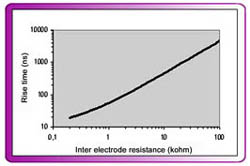
Figure 2. The rise time of a PSD can be changed by several orders of magnitude by varying the inter electrode resistance.
Size and shape
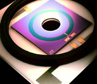
Not only electro-optical parameters can be tuned to fit the customers needs but also the size and the shape of the device. The size can be varied almost endlessly. Short, wide devices as well as long, narrow ones are possible. Only the starting material sets the limit.
The shape is also variable. During our 26 years, SiTek has custom designed not only rectangular and square devices, but a large number of odd shaped PSDs as well. These include circular, trapezoidal and sector shaped ones.
So, as you can see from these two articles on custom design processing, there is a lot that can be done in order to optimise the performance of the PSD for a specific application. SiTek supply such PSDs to satisfied customers worldwide and our versitility means that we can always find the best solution for your needs.
« home