
![]()
News
Investment Increasing Quality
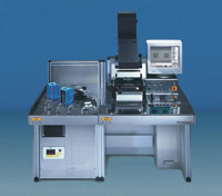 SiTek is well known for having the shortest delivery times of all PSD manufacturers, especially on custom designed products. To ensure that we can keep our short delivery times also with the increasing demand we see on our products a continuous work on our production line automation is on-going. We have now taken the next step in this process by the purchasing of a fully automatic mask aligner, EV620 from EV Group in Austria.
The manufacturing of the PSD chips is, like most semiconductor device manufacturing, done by adding layers of materials to a semiconductor wafer until the final structure has been created. Each layer has its special purpose, e.g. active area, metal contacts etc, and it needs an individual pattern to work properly. This pattern is defined by a mask aligner. Since the functionality of the complete PSD is build by the interaction between all these layers it is of greatest importance that the patterns of the layers are accurately aligned to each other. In fact, for some of our devices, the alignment between layers has to be done with an accuracy of only a few microns to fulfil the demands on functionality our customers have.
To manufacture the duo-lateral high linearity PSD, that SiTek does, puts an even higher demand on the alignment. This is because the patterns on the back side must be aligned to the ones on the front as well, with the same high accuracy.
As the PSD chip is built by several layers, each wafer will pass through the patterning stage numerous times during the manufacturing process. Hence, it is not only important with high alignment accuracy but also with high through-put.
A mask aligner that fulfils all these demands is the EV620 from the Austrian manufacturer EV Group. The high through-put is ensured by the robot wafer handling as well as the automatic alignment feature and the high accuracy is obtained by an advanced automatic pattern recognition system. The robot handling is not only favourable from a through-put point of view, but also from a quality point of view. Manual wafer handling always increases the risk for particle contamination and by introducing the fully automatic robot handling system the manual handling is kept to minimum during this critical process step. Since the new mask aligner not only increases the capability in terms of through-put but also pushes the accuracy and resolution into the sub-micron region, our possibilities for further PSD developments has also increased. With the new mask aligner we have put ourselves in a good position for the future and made us well prepared to meet the increased demands on our PSDs both from customers as well as applications.
« home