
News
Visiting the 'Float Zone'
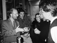
On November 10, 1999, SiTek paid an interesting visit to our wafer supplier Topsil Semiconductor Material A/S in Denmark.
Our objective was to learn about silicon the base material for our production. Topsil´s Sales and Marketing manager as well as the Production manager welcomed us and gave us a good tour of the facilities.
 Silicon is a fascinating semiconductor material. It is the second most common material
on earth after oxygen.In order to produce state of the art high quality detectors
SiTek uses only the purest silicon of all, the Float Zone (FZ) silicon.
Silicon is a fascinating semiconductor material. It is the second most common material
on earth after oxygen.In order to produce state of the art high quality detectors
SiTek uses only the purest silicon of all, the Float Zone (FZ) silicon.Topsil is one of the world´s leading supplier of this kind of silicon with more than 40 years business experience. Silicon is abundantly available in ordinary sand but as we all know sand is not a very clean material. It will take several steps of purification before this silicon is transferred into poly-silicon ingots, a form of material suitable for wafer manufacture.
For this material to be useful for electronic components, however, the crystal structure in the material has to be invariant through the whole ingot, in other words the ingot has to be one large crystal contrary to the poly-silicon which is composed of a large number independent crystals. To achieve this Topsil uses the Floating Zone technique for the crystal conversion. That means that poly-silicon is melted by a high frequency induction coil. At the bottom of the melt a mono-crystalline seed crystal is introduced.
This seed will work as a template for the arrangement ofthe crystal lattice as the molten zone is " floated" along the entire length of the poly ingot. The end result is a mono-crystal FZ-ingot. Adding phosphorous or boron contented gas to the molten zone controls the electrical properties of final silicon. When the single crystal has been "pulled" it is cut into wafers. Here we had the opportunity to watch the Topsil's new wire-cutter in action. This high capacity machine uses a set of parallel wires to slice the ingot into wafers with high accuracy and similarity. Needless to say, the surfaces of the new cut wafers are very raw, and several steps of lapping, etching and polishing is needed before the wafers get the smooth, highly reflective, mirror-like surface we are used to SiTek. Each wafer has to be absolutely free from contamination, particles and microscopic damages, so the final processing and inspection will take place in a clean room environment.
Topsil is at the front edge of FZ technology. An accomplishment that has been record and recognised by SiTek and that very well suits our commitment to quality. We will be looking forward to a continued close partnership with our #1 silicon supplier.
« home